


Optical light sources
Optical light sources
Optical light sources simulate the optical voice, video and data signals of real-life service applications, making them an essential component of a thorough testing process. An optical light source (laser, LED, etc.) is used to emit electromagnetic radiation in order to perform a specific task, whether detecting faults, breaks and microbends, characterizing link-loss or certifying LAN/WANs. As recommended by the ITU-T (G.983.3), optical light sources are also used to test PON networks at three different wavelengths (1310/1490/1550 nm).
The principal light sources used for Optical Sources optic communication application are heterojunction-structured semiconductor laser diodes (also referred to as injection laser diodes or ILDs) and light-emitting diodes (LEDs). A heterojunction consists of two adjoining semiconductor materials with different band-gap energies. These devices are suitable for fiber transmission systems because they have adequate output power for a wide range of applications, their optical power output can be directly modulated by varying the input current to the device, they have a high efficiency, and their dimensional characteristics are compatible with those of the optical fiber. Comprehensive treatments of the major aspects of LEDs and laser diodes are presented in various books and review articles.
The intent of this chapter is to give an overview of the pertinent characteristic of fiber-compatible luminescent sources. The first section discusses semiconductor material fundamentals that are relevant to light source operation. The next two sections present the output and operating characteristics of LEDs and laser diodes, respectively. These are followed by sections discussing the temperature responses of optical sources, their linearity characteristics, and their reliability under various operating conditions.
We shall see in this chapter that the light-emitting region of both LEDs and laser diodes consists of a p n junction constructed of direct-band-gap III-V semiconductor materials. When this junction is forward biased, electrons and holes are injected into the p and n regions, respectively. These injected minority carriers can recombine either radiatively, in which case a photon of energy hv is emitted, or nonraiatively, whereupon the recombination energy is dissipated in the form of heat. This pn junction is thus known as the active or recombination region.
A major difference between LEDs and laser diodes is that the optical output from an LED is incoherent. Whereas that from a laser diode is coherent. In a coherent source, the optical energy is produced in an optical resonant cavity. The optical energy released from this cavity has spatial and temporal coherence, which means it is highly monochromatic and the output beam is very directional. In an incoherent LED source, no optical cavity exists for wavelength selectivity. The output radiation has a broad spectral width, since the emitted photon energies range over the energy distribution of the recombining electrons and holes, which usually lie between 1 and 2kBT (kB is Boltzmann’s constant and T is the absolute temperature at the pn junction). In addition, the incoherent optical energy is emitted into a hemisphere according to a cosine power distribution and thus has a large beam divergence.
In choosing an optical source which is compatible with the optical waveguide, various characteristics of the fiber, such as its geometry, its attention as a function of wavelength, its group delay distortion (bandwidth), and its modal characteristics, must be taken into account. The interplay of these factors with the optical source power, spectral width, radiation pattern, and modulation capability needs to be considered. The spatially directed coherent optical output from a laser diode can be coupled into either single-mode or multimode fibers. In general, LEDs are used with multimode fibers, since normally it is only into a multimode fiber that the incoherent optical power from an LED can be coupled in sufficient quantities to be useful. However, LEDS have been employed in high-speed local-area applications in which one wants to transmit several wavelengths on the same fiber. Here, a technique called spectral slicing is used.13-15this entails using a passive device such as waveguide grating array (see chapter 10) to split the broad spectral emission of the LED into narrow spectral slices. Since these slices are each centered at a different wavelength, they can be individually modulated externally with independent data streams and simultaneously sent on the same fiber.
Topics from semiconductor physics
Since material in this chapter assumes a rudimentary knowledge of semiconductor physics, various relevant definitions are given here for semiconductor material properties, including the concepts of energy brands, intrinsic and extrinsic materials, pn junctions, and direct and indirect band gaps. Further details can be found in Refs. 16-18.
Energy bands
Semiconductor materials have conduction properties that lie somewhere between those of metals and insulators. As an example material, we consider silicon (Si), which is located in the fourth column (group IV ) of the periodic table of elements. A Si atom has four electrons in its outer shell, by which it makes covalent bonds with its neighboring atoms in a crystal. Such outer-shell electrons are called valence electrons. Optical Sources
The conduction properties of a semiconductor can be interpreted with the aid of the energy-band . in a semiconductor the valence electrons occupy a band of energy levels called the valence band. This is lowest band of allowed states. The next higher band of allowed energy levels for the electrons is called the conduction band. In a pure crystal at low temperature, the conduction band is completely empty of electrons and the valence band is completely full. These two bands are separated by an energy gap, in which no energy levels exit. Optical Sources As the temperature, the conduction band is completely empty of electrons and the valence band is completely full. These two bands are separated by an energy gap, in which no energy levels exist. As the temperature is raised, some electrons are thermally excited across the band gap. For Si this excitation energy must be greater than 1.1 eV, which is the band-gap energy. This gives rise to a concentration n of free electrons in the conduction band, which leaves behind and equal concentration p of vacancies, or holes, in the valence band, as is shown schematically . Both free electrons and holes are mobile within the material, so that both can contribute to electrical conductivity; that is, an electron in the valence band can move into a vacant hole. This action makes the hole move in the opposite direction to the electron flow.
When an electron propagates in the semiconductor, it interacts with the periodically arranged constituent atoms of the material and thus experiences external forces. As a result, to describe its acceleration acrys in a semiconductor crystal under an external force F ext its mass needs to be described by a quantum mechanical quantity me called the effective mass. That is, when using the relationship Fext = meacrys (force equals mass times acceleration),the effects of all the forces exerted on the electron within the material are incorporated into me.
The concentration of electrons and holes is known as the intrinsic carrier concentration ni, and for a perfect material with no imperfections or impurities it is given by
n = p= ni = K exp
where
K = 2(2πkBT/h2)3/2(memh)3/4
is a constant that is characteristic of the material. Here, T is the temperature in degrees kelvin, KB is Boltzmann’s constant, h is Planck’s constant, and me and mh are the effective masses of the electrons and holes, respectively, which can be smaller by a factor of 10 or more than the free-space electron rest mass of 9.11×10⁻³¹kg
The conduction can be greatly increased by adding traces of impurities from the group V elements (e.g.,P,As, Sb). This process is called doping and the doped semiconductor is called an extrinsic material. These elements have five electrons in the outer shell. When they replace a Si atom, four electrons are used for covalent bonding , and the fifth, loosely bound electron is available for conduction. As a, this gives rise to an occupied level, just below the conduction band, called the donor level. The impurities are called donors because they can give up an electron to the conduction Band. This is reflected by the increase in the free-electron concentration in the conduction band, as. Since in this type of material the current is carried by ( negative) electrons (because the electron concentration is much higher than that of holes), it is called n-type material.
The conduction can also be incrased by adding group III elements, which have three electrons in the outer shell. In this case, three electron is created. As a, this gives rise to an unoccupied level just above the valence band. Conduction occurs when electrons are excited from the valence band to this acceptor level (so called because the impurity atoms have accepted electrons from the valence band). Correspondingly, the free-hole concentration increases in the valence band. This is called p-type material because the conduction is a result of (positive) hole flow.
Intrinsic and Extrinsic Material
A perfect material containing no impurities is called an intrinsic material. Because of thermal vibrations of the crystal atoms, some electrons in the valence band gain enough energy to be excited to the conduction band. This thermal generation process produces free electron-hole pairs, since every electron that moves to the conduction band leaves behind a hole. Thus, for an intrinsic material the number of electrons and holes are both equal to the intrinsic carrier density, as denoted by Eq. In the opposite recombination process, a free electrons releases its energy and drops into a free hole in the valence band. For an extrinsic semiconductor, the increase of one type of carrier reduces the number of the other type. In this case, the product of the two types of carriers remains constant at a given temperature. This gives rise to the mass-action law
Pn=ni2
Which is valid for both intrinsic and extrinsic materials under thermal equilibrium Structure. The junction between the two material regions, which is known as the pn junction, is responsible for the useful electrical characteristics of a semiconductor device.
When a pn junction is created, the majority carriers diffuse across it. This causes electrons to fill holes in the p side of the junction and causes holes to appear on the n side. As a result, an electric field (or barrier potential) appears across the junction, this field prevents further net movements of charges once equilibrium has been established. The junction area now has no mobile carriers, since its electrons and holes are locked into a covalent bond structure. This region is called either the depletion region or the space charge region.
When an external battery is connected to the pn junction with its positive terminal to the n-type material and its negative terminal to the p-type material, the junction is said to be reverse-biased. As a result of the reverse bias, the width of the depletion region will increase on both the n side and the p side. This effectively increase on both the n side and the p side. This effectively increases the barrier potential and prevents any majority carriers from flowing across the junction. However, minority carriers can move with the field across the junction. The minority carrier flow is small at normal temperatures and operating voltages, but it can be significant when excess carriers are created as, for example, in an illuminated photodiode.
When the pn junction is forward-biased, the magnitude of the barrier potential is reduced. Conduction-band electrons on the n side and valence-band holes on the p side are, thereby, allowed to diffuse across the junction. Once across, they significantly increase the minority carrier concentrations, and the excess carriers then recombine with the oppositely charged majority carriers. The recombination of excess minority carriers is the mechanisms by which optical radiation is generated.
Direct and Indirect Band Gaps – Optical Sources
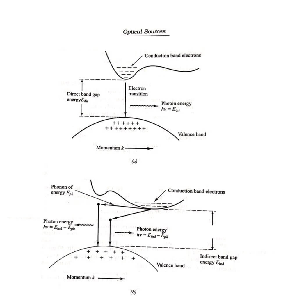
In order for electron transitions to take place to or from the conduction band with the absorption or emission of a photon, respectively, both energy and momentum must be conserved. Although a photon can have considerable energy, its momentum hv/c is very small.
Semiconductors are classified as either direct-band-gap or indirect-band-gap materials depending on the shape of the band gap as a function of the momentum k,. Let us consider recombination of an electron and a hle, accompanied by the emission of a photon. The simplest and most probable recombination process will be that where the electron and hole have the same momentum value . This is a direct-band-gap material.
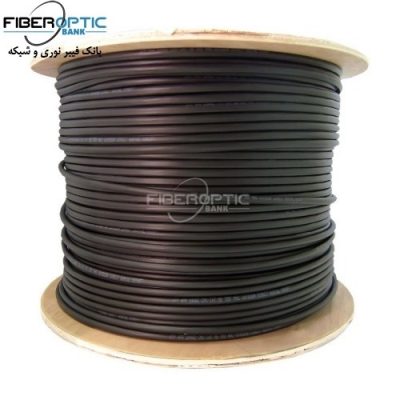
For indirect-band-gap materials, the conduction-band minimum and the valence-band maximum energy levels occur at different values of momentum, as shown in image. Here, band-to-band recombination must involve a third particle to conserve momentum, since the photon momentum is very small. Phonons (i.e., crystal lattice vibrations) serve this purpose.
Semiconductor Device Fabrication
In fabricating semiconductor devices, the crystal structure of the various materials regions must be carefully taken into account. In any crystal structure, single atoms (e.g., Si or Ge) or groups of atoms (e.g., NaCl or GaAs) are arranged in a repeated pattern in space. This periodic arrangement defines a lattice,and the spacing between the atoms or groups of atoms is called the lattice spacing or the lattice constant. Typical lattice spacings are a few angstroms.
Semiconductor devices are generally fabricated by starting with a crystalline substrate which provides mechanical strength for mounting the device and for making electric contacts. A technique of crystal growth by chemical reaction is then used to grow thin layers of semiconductor materials on the substrate. These materials must have lattice structures that are identical to those of the substrate crystal. In particular, the lattice spacings of adjacent materials should be closely matched to avoid temperature-induced stresses and strains at the material interfaces. This types of growth is called epitaxial, which is derived from the Greek words epi meaning ‘on” and taxis meaning “arrangement”; that is, it is an arrangement of atoms from one material on another material. An important characteristic of epitaxial growth is that it is relatively simple to change the impurity concentration of successive material layers, so that a layered semiconductor device can be fabricated in a continuous process. Epitaxial layers can be formed by growth techniques of either vapor phase, liquid phase, or molecular beam.
Light-Emitting Diodes (LEDs)
For optical communication systems requiring bit rates less than approximately 100-200 Mb/s together with multimode fiber-coupled optical power in the tens of microwatts, semiconductor light-emitting diodes (LEDs) are usually the best light sources choice. These LEDs require less complex drive circuitary than laser diodes since no thermal or optical stabilization circuits are needed (sec Sec.4.3.6), and they can be fabricated less expensively with higher yields.
LED Structures – Optical Sources
To be useful in fiber transmission applications an LED must have a high radiance output, a fast emission response time, and a high quantum efficiency. Its radiance (or brightness) is a measure, in watts of the Optical Sources power radiated into a unit solid angle per unit area of the emitting surface. High radiances are necessary to couple sufficiently high optical power levels into a fiber, detail in Chapter 5. The emissions response time is the time delay between the applications of a current pulse and the onset of optical emission. As we discuss in Secs 4.2.4 and 4.3.7, this time delay is the factor limiting the bandwidth with which the source can be modulated directly by varying the injected current. The quantum efficiency is related to the fraction of injected electron-hole pairs that recombine radiatively. This is defined and described in detail in Sec. 4.2.3.
To achieve a high radiance and a high quantum efficiency, the LED structure must provide a means of confining the charge carriers and the stimulated optical emission to the active region of the pn junction where radiative recombination takes place. Carrier confinement is used to achieve a high level of radiavite recombination in the active region of the device, which yields a high quantum efficiency. optical confinement is of importance for preventing absorption of the emitted radiation by the material surrounding the pn junction.
To achieve carrier and Optical Sources confinement, LED configuration such as homojunctions and single and double heterojunctions have been widely investigated. The most effective of these structures is the configuration. This is referred to as a double-heterostructure (or heterojunction) device because of the two different alloy layers on each side of the active region. This configuration evolved from studies on laser diodes. By means of this sandwich structure of differently composed alloy layers, both the carriers and the and the optical field to the central active layer. The band-gap differences of adjacent layers confine the charge carriers, while the differences in the indices of refraction of adjoining layers confine the optical field to the central active layer. This dual confinement leads to both high efficiency and high radiance. Other parameters influencing the device performance include optical absorption in the active region (self-absorption), carrier recombination at the heterostructure interfaces, doping concentration of the active layer, injection carrier density, and active-layer thickness. Optical Sources We shall see the effects of these parameters in the following sections.
The two basic LED configurations being used for fiber optics are surface emitters (also called Burns or front emitters) and edge emitters20. In the surface emitter, the plane of the active light-emitting region is oriented perpendicularly to the axis of the fiber. In this configuration, a well is etched through the substrate of the device, into which a fiber is then cemented in order to accept the emitted light. The substrate of the device, into which a fiber is then cemented in order to accept the emitted light. The circular active area in practical surface emitters is nominally 50µm in diameter and up to 2.5µm thick. The emission pattern is essentially isotropic with a 1200 half-power beam width.
This isotropic pattern from a surface emitter is called a lambertian pattern. In this pattern, the source is equally bright when viewed from any direction, but the power diminishes as cos θ, where θ is the angle between the viewing direction and the normal to the surface (this is because the projected area one sees decreases as cos θ). Thus, the power is down to 50 percent of its peak when θ=600, so that the total half-power beam width is 1200.
The edge emitter depicted consists of an active junction region, which is the source of the incoherent light, and two guiding layers. The guiding layers both have a refractive index which is lower than that of the active region but higher then the index of the surrounding material. Optical Sources This structure forms a waveguide channel that directs the Optical Sources radiation toward the fiber core. Optical Sources To match the typical fiber-core diameter (50-100µm), the contact stripes for the edge emitter are 50-70µm wide. Lengths of the active regions usually range from 100 to 150 µm. The emission pattern of the edge emitter is more directional than that of the surface emitter, as is illustrated. In the plane parallel to the junction, where there is no waveguide effect, the emitted beam is lambertian (varying as cos θ) with a half-power width of θ11=1200. In the plane perpendicular to the junction, the half-power beam θ1 has been made as small as 25-350 by a proper choice of the waveguide thickness2,20.
Source:
Related products...
fiber-optic-cable
fiber-optic-cable
[ratings]